

服务热线:0755- 83387360
 产品介绍
产品介绍
The SN74LVC126A device is a quadruple bus buffer gate designed for 1.65-V to 3.6-V VCC operation. The SN74LVC126A device features independent line drivers with 3-state outputs. Each output is disabled when the associated output-enable (OE) input is low. To ensure the high-impedance state during power up or power down, OE must be tied to GND through a pulldown resistor; the minimum value of the resistor is determined by the current-sourcing capability of the driver. Inputs can be driven from either 3.3-V or 5-V devices. This feature allows the use of this device as a translator in a mixed 3.3-V and 5-V system environment.
 订购信息
订购信息
| 器件类目 | 产品型号 |
封装 |
工作温度 |
是否在产 | 应用 | 丝印 |
| 缓冲器 | SN74LVC126APWR |
TSSOP14 |
–40~+125°C |
是 |
AV接收器、便携式音频设备、MP3、无线耳机、键盘、鼠标
|
LC126A |
 引脚配置与功能

 产品特性
产品特性
Operates From 1.65 V to 3.6 V
Specified From –40°C to +125°C
Inputs Accept Voltages up to 5.5 V
Maximum tpd of 4.7 ns at 3.3 V
Typical VOLP (Output Ground Bounce)
Latch-Up Performance Exceeds 250 mA Per JESD 17
 应用范围
应用范围

原装现货,技术选型

云仓现货,快速配送

品类齐全,性能优良

工厂直销,样品申请

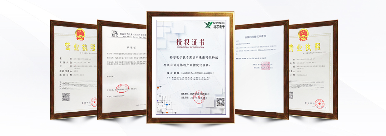
 荣誉资质
荣誉资质
